STM32F103 Development Board---- STM32F103RCT6
● STM32F103 development board (STM32F103RCT6) introduction
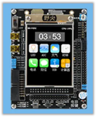
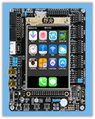
The STM32F103 development board (STM32F103RCT6) also known as stm32f103rct6 development board or stm32f103 minimum development board, it is an integrated circuit board that uses STM32F103RCT6 as the main control chip. It is a hardware learning platform for learning the software development and hardware development of the STM32F103RCT6 microcontroller.
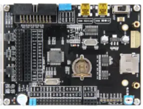
STM32F103RCT6 development board not only integrates onboard resources such as clock, buzzer, ISP (serial download), etc., but also has rich peripheral interfaces, which can external wireless, Bluetooth, infrared modules to achieve specific functions.
The STM32F103RCT6 development board is a basic learning board, it is the primary version of the stm32f103 development board series which can realize basic functions and meet basic requirements. It has simple functions and is easy to use. For beginners, the STM32F103RCT6 development board is a good choice.
STM32F103 series development boards (including STM32F103RCT6 development board, STM32F103VET6 development board, STM32F103ZET6 development board) are the best STM32 development board for beginners.
● 8051 development board datasheet
1.Ultra-low price.
Getting 32-bit products at the price of 8-bit is the biggest advantage of the STM32F103 development board.
2.Abundant peripheral interfaces.
This development board has various peripheral interface, can be connected to wireless, Bluetooth, infrared, temperature control and other modules.
3.The STM32F103 development board uses STM32F103RCT6 as the main chip, the CPU operating frequency is up to 72 MHz, and there are 64 pins and 51 io ports.
This development board makes the best use of this chip for teaching, so that beginners can learn more knowledge.
4.The onboard resource module is simple and easy to use, which is a good choice for beginners.
5.The STM32F103 development board has a one-click download function onboard.
The download of the program can be completed through a USB data line, and the communication and download can be realized through a USB-to-serial interface.
● STM32F103 development board datasheet -----STM32F103 development board (STM32F103RCT6) hardware configuration checklist
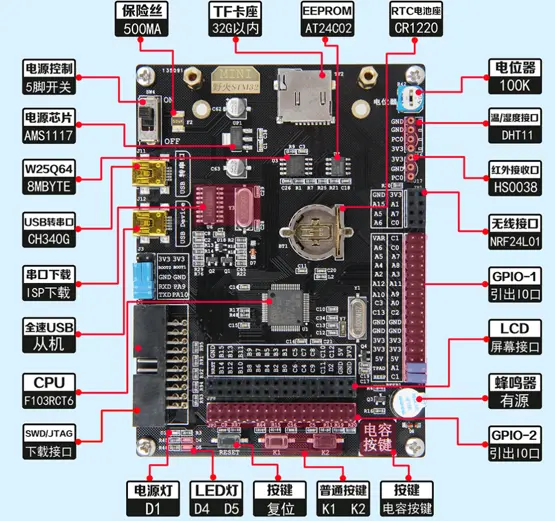
| Size | 109*80mm |
|---|---|
| PCB | 2 layers, black immersion gold |
| CPU | STM32F103RCT6, 64PIN, 256K FLASH, 48K SRAM, 2 of 16-bit basic timers, 4 of 16-bit general-purpose timers, 2 of 16-bit advanced timers, 2 of DMA controllers, 3 of SPI, 2 of IIC, 5 of Serial port, 1 of USB, 1 of CAN, 3 of 12-bit ADC, 1 of 12-bit DAC, 1 of SDIO interface, 51 of general IO ports. |
| Bluetooth | It can be connected with HCO5 Bluetooth module, cooperate with APP can realize Bluetooth wireless control |
| Wireless | It can be connected with 2.4G wireless NRF24L01 module to realize wireless communication function. Note: NRF24L01 communication requires at least 2 modules and 2 development boards to work at the same time to achieve wireless communication. |
| FLASH | Model: W25Q64, capacity 8M bytes (64M bit). Can store some infrequently modified data such as fonts, etc., thus greatly saving the occupancy of STM32 internal FLASH. |
| EEPROM | Model: AT24C02, storage capacity of 256 bytes, with the function of no power loss, usually very important data is stored in this chip, such as touch screen calibration parameters, etc. |
| SD card | It can expand the TF card within 32GB (including 32GB), which can be used for external expansion of storage capacity and other applications |
| RTC transposon | 1 of CR1220 battery holder to maintain the storage of data in the backup area and the operation of the RTC clock |
| Power input | USB 5V input |
| Power chip | Power regulator chip, model: AMS1117-3.3. Because STM32 is powered by 3.3V, we need to convert the 5V voltage of USB to 3.3V. This chip is a linear voltage regulator chip that converts 5V to 3.3V. Effectively prevent the chip from burning out. |
| Fuse | 1 of 500MA resettable fuse |
| Buzzer | 1 of active buzzer, which can be used for applications such as alarm prompts or making music boxes |
| Potentiometer | 1 of 100K precision SMD potentiometer |
| Key | 1 of reset key, 2 of ordinary keys, 1 of capacitive key, total 4 keys, among which K_UP can be used as standby wake-up function. It is used for applications such as adjustment and control of some parameters. Two common keys can be used for human-computer interaction input. |
| LED | 2 LEDs, 1 power LED, and 2 LEDs are labeled on the development board: D4 and D5. D4 is red, D5 is green, mainly for the convenience of identification. |
| Liquid crystal (LCD) | It can be connected to 3.2 inch resistive screen, 5 inch capacitive screen. Can be used for liquid crystal display(LCD) project development, such as human-machine touch screen, advertising machine, etc. |
| Serial port | 1 of USB to serial port (CH340), which can realize USB download code, serial communication, etc. |
| USB | 1 of USB-device interface, which can realize USB communication. |
| Download | ①:total 2 download interfaces, 1 SWD interface, 1 JTAG interface, both download and debug program interfaces. |
| ②:Support emulators such as DAP/JLINK/ULINK2/ST-LINK/ARM-OB etc. | |
| ③:Support serial ISP one-click download | |
| Temperature and humidity | Connect to external temperature and humidity sensor DHT11 module, to check the temperature and humidity. |
| Infrared | Can be connected to HS0038 infrared receiver, for various control applications such as infrared communication, can receive infrared signals sent by remote control |
| GPIO | SDIO, total of 112 GPIO (PA/PB/PC..PG) are convenient for users to develop other modules |
| SPl1 and SPI2, serial peripheral interface, it can make the microcontroller communicate with various peripheral devices in a serial manner to exchange information. Peripherals include Flash RAM, network controller, LCD display driver, A/D converter and MCU, etc. | |
| I2C1 and I2C2, used to connect the microcontroller and the peripheral device serial communication mode | |
| USART 1/2/3, Universal Synchronous Asynchronous Transceiver Transmitter. The working principle is to transmit each character of the transmitted data bit by bit, it can convert the data to be transmitted between serial communication and parallel communication, and can flexibly exchange full-duplex data with external devices. |
● STM32F103 development board schematic (STM32F103RCT6 )
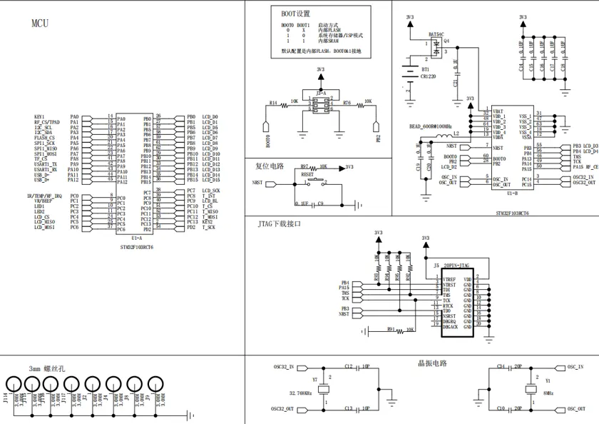
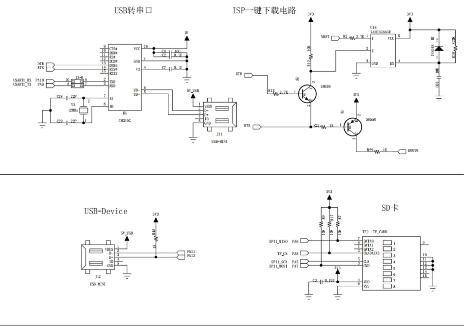
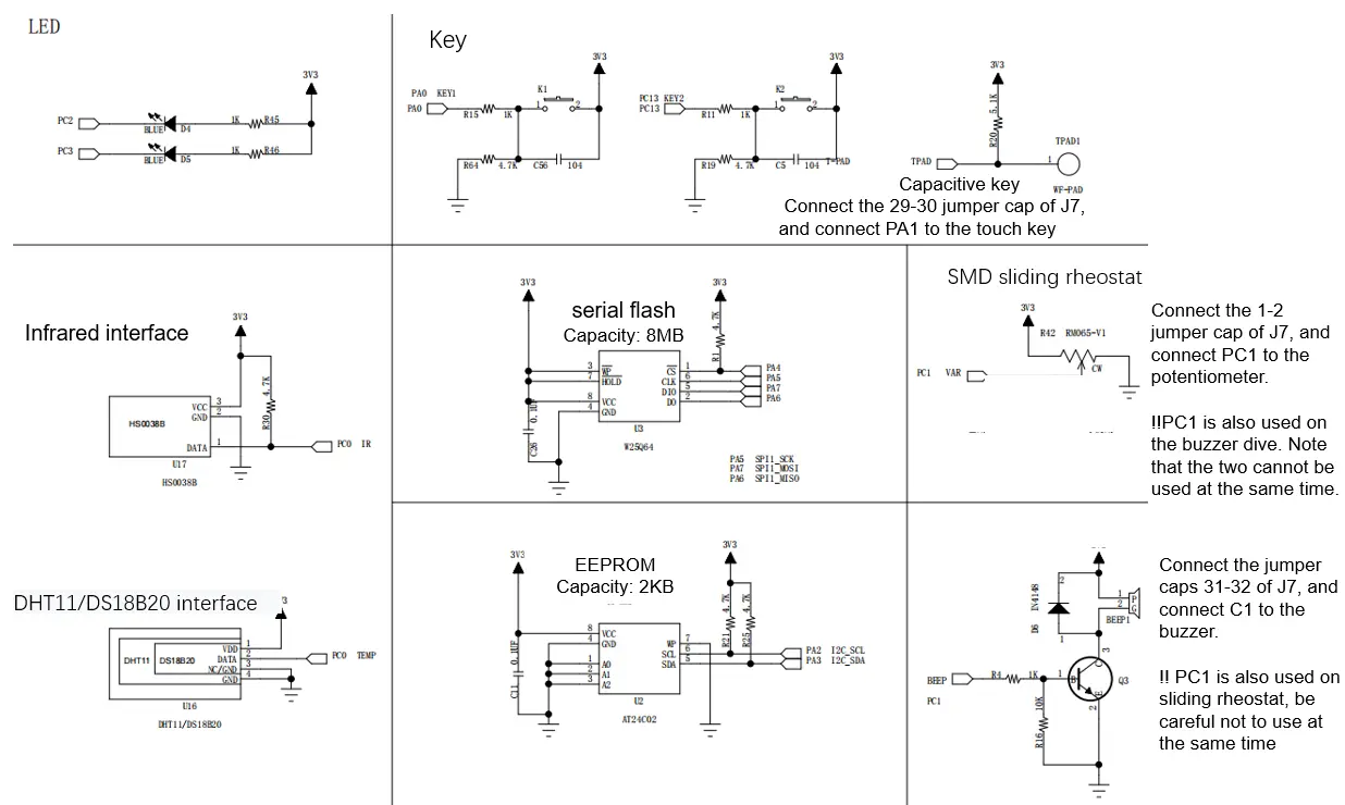
● STM32F103 development board schematic (STM32F103RCT6 ) experimental examples
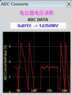
Experiment 1: ADC module function
The ADC module converts the analog voltage signal into a digital signal that the CPU can process. The STM32F103RCT6 development board is used with an ADC module and a potentiometer to collect voltage. When the potentiometer is rotated, the voltage changes accordingly, and the ADC module displays the changed voltage in the form of a waveform and turns it into a digital signal that we can understand.
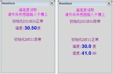
Experiment 2: Temperature and Humidity Module Function
The Humiture APP can be used to display detected temperature and humidity data. The stm32f103 minimum development board is connected to a DS18B20 temperature sensor or a DHT11 temperature and humidity sensor, which can detect temperature and humidity data.
Temperature and humidity sensor to be purchased separately
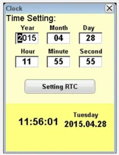
Experiment 3: RTC clock function
The Clock APP uses the RTC function of the stm32f103 minimum development board. You need to put a button battery into the battery holder on the STM32F103RCT6 development board. The RTC clock of the STM32F103RCT6 development board will continue to run after the main power supply is cut off. Turn on the Clock next time. You will see the update time in the APP. (The battery holder is below the LCD screen, the battery model is: CR1220)
Experiment 4: Mobile phone communication function
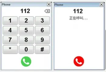
PHONE is a phone dialing application. The STM32F103 development board schematic (STM32F103RCT6 ) can be used with an external GSM module (requires access to a SIM card) to realize the mobile phone communication function. The wiring method is shown in the figure below (the GSM module needs to be purchased separately, click to view)
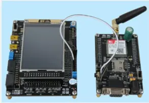
GSM module and development board connection diagram
● STM32F103 development board schematic (STM32F103RCT6 ) shipping standard list

Qty.:1

Qty.:2

Qty.:1

Qty.:1
Please kindly note, it is not equipped with LCD screen, if you need it, please buy it separately
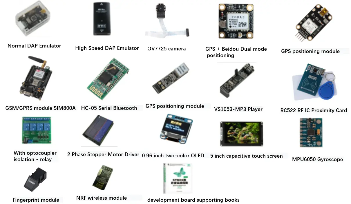
● Modules that can be connected to the STM32F103 development board schematic (STM32F103RCT6 )
The STM32F103 development board schematic (STM32F103RCT6 ) can also be connected to many other modules and can be purchased as needed, all with preferential prices.
